Tunnelling Contact Helps to Study Electron Structure of Carbon Nanotubes

Russian physicists have demonstrated how tunnelling contacts can be used for single-particle states spectroscopy in carbon nanotubes. The proposed technology of tunnelling contact fabrication and the spectroscopic method will help measure the exact nanotube bandgap value, which is the key characteristic required for design of any nanotubes-based electronic devices. Applied Physics Letters publishes the result of the study.
Carbon nanotubes are unique entities in their physical nature and properties. They have been researched extensively over the past three decades and have applications in various fields of science and technology, including materials studies, physics, and electronics, to name but a few.
A carbon nanotube can be compared to a rolled graphene sheet. The properties of carbon nanotubes are truly unique, as the way in which this sheet is rolled up determines the bandgap width, which, in turn, determines the semiconducting or metallic properties of a nanotube. Consider an ordinary piece of paper: it can easily be rolled up into a tube by joining either two opposite sides or two opposite corners; alternatively, one corner can be joined to any point on the opposite side. The properties of a sheet of paper do not depend on exactly how it is rolled up. If we now replace the sheet of paper with a small piece of graphene it turns out that it will behave either like a semiconductor or like a metal in terms of its conductivity depending on which way we rolled the graphene into a tube. This behaviour makes carbon nanotubes a very attractive material for building all sorts of electronic devices.
The bandgap width is the main characteristic of semiconductors, which is primarily responsible for their applications. At this stage of technological development, no good method for growing carbon nanotubes with known bandgap widths has yet been devised. The synthesis process can produce carbon nanotubes with varying bandgaps, or even no bandgap at all. To determine the bandgap width and the specific type of electron energy distribution, tunnelling spectroscopy has traditionally been used for each individual tube using a tunnelling microscope. This method has a number of disadvantages; it is imprecise, expensive, and non-technological.

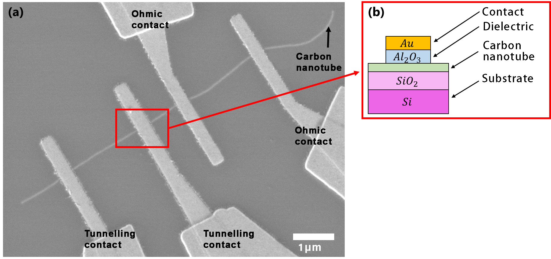
In the published study, researchers proposed a technologically advanced (ie, highly compatible with current electronics fabrication techniques) and scalable method to determine the electron spectrum of an individual carbon nanotube. The researchers fabricated a tunnelling contact (see Figure (a)), which is a contact with a very high electrical resistance. Rather than directly, the metal of the contact interacts with the tube through a thin dielectric layer (see Figure (b)).
‘The dielectric creates a tunnel barrier, an energy wall that prevents transfers of charge carriers. A “classical” particle cannot cross such a barrier, but quantum mechanics “allows” a conduction electron or a hole to pass through the barrier, or to “tunnel”. It is worth noting that the probability of tunnelling is proportional to the density of states in the object under study. Because of this property, tunnelling contacts allow for scanning electron energy distribution in the tube,’ says Yakov Matyushkin, one of the study's authors, a Junior Research Fellow at the MIPT Laboratory of Nanocarbon Materials and a HSE MIEM research assistant and doctoral student.
The researchers made a series of samples, each of which was a single carbon nanotube with two pairs of ohmic and two pairs of tunnel contacts (see Figure (a)). The researchers first grew the tube on a silicon substrate. After that, they attached the tunnelling and ohmic contacts to it. During the experiment, voltage was applied between the tunnelling contact and the ohmic contact at the temperature of liquid helium and the electric current, which flowed through the system was measured. The dependence of the current on the voltage made it possible to obtain the electron spectrum in a carbon nanotube and determine the bandgap width.

Georgy Fedorov
'The proposed method provides information about the band structure of carbon nanotubes. It also helps in determining how this structure changes under the influence of external factors. For instance, we observed the removal of valence degeneracy in a magnetic field using tunnelling contact. This long-predicted effect manifests itself in energy splitting of state density maxima. This is the first time we have demonstrated this effect in an individual nanotube,’ says co-author Georgy Fedorov, Deputy Head of the MIPT Laboratory of Nanocarbon Materials.
The samples were made by the MIPT Laboratory of Nanocarbon Materials based on the MIPT Shared Facility Centre. The experiments were carried out by the Radiophysics Laboratory, Moscow State Pedagogical University, and by the MIPT Shared Facility Centre for Studies of HTS and other Strongly Correlated Materials (SFC LPI).'
The research was supported by the Russian Foundation for Basic Research, the Russian Science Foundation, and the Russian Ministry of Education and Science.
Yakov Matyushkin
See also:
Russian Scientists Reconstruct Dynamics of Brain Neuron Model Using Neural Network
Researchers from HSE University in Nizhny Novgorod have shown that a neural network can reconstruct the dynamics of a brain neuron model using just a single set of measurements, such as recordings of its electrical activity. The developed neural network was trained to reconstruct the system's full dynamics and predict its behaviour under changing conditions. This method enables the investigation of complex biological processes, even when not all necessary measurements are available. The study has been published in Chaos, Solitons & Fractals.
Russian Physicists Discover Method to Increase Number of Atoms in Quantum Sensors
Physicists from the Institute of Spectroscopy of the Russian Academy of Sciences and HSE University have successfully trapped rubidium-87 atoms for over four seconds. Their method can help improve the accuracy of quantum sensors, where both the number of trapped atoms and the trapping time are crucial. Such quantum systems are used to study dark matter, refine navigation systems, and aid in mineral exploration. The study findings have been published in the Journal of Experimental and Theoretical Physics Letters.
Russian Scientists Demonstrate How Disorder Contributes to Emergence of Unusual Superconductivity
Researchers at HSE University and MIPT have investigated how the composition of electrons in a superconductor influences the emergence of intertype superconductivity—a unique state in which superconductors display unusual properties. It was previously believed that intertype superconductivity occurs only in materials with minimal impurities. However, the scientists discovered that the region of intertype superconductivity not only persists but can also expand in materials with a high concentration of impurities and defects. In the future, these superconductors could contribute to the development of highly sensitive sensors and detectors. The study has been published in Frontiers of Physics.
Scientists at HSE University Devise More Accurate Method for Predicting the Electrical Conductivity of Electrolyte Solutions
Researchers at HSE MIEM have developed a model for calculating the electrical conductivity of aqueous electrolyte solutions; for the first time, it considers the spatial distribution of ion charges instead of assuming their localisation at a single point. The model remains effective even at high electrolyte concentrations and across a wide temperature range. This breakthrough will contribute to the development of more efficient batteries and enable the calculation of electrical conductivity without the need for experimental testing. The study has been published in the Journal of Chemical Physics.
Russian Scientists Integrate Microdisk Laser and Waveguide on a Single Substrate
A group of Russian scientists led by Professor Natalia Kryzhanovskaya at HSE Campus in St Petersburg has been researching microdisk lasers with an active region based on arsenide quantum dots. For the first time, researchers have successfully developed a microdisk laser coupled with an optical waveguide and a photodetector on a single substrate. This design enables the implementation of a basic photonic circuit on the same substrate as the radiation source (microlaser). In the future, this will help speed up data transfer and reduce equipment weight without compromising quality. The study results have been published in Semiconductors.
First Successful Attempt in 55 years: Physicists in Russia and Germany Confirm 1969 Experiment Results
A team of researchers, with the participation of physicists from HSE University, replicated the 1969 experiment on superconductivity and its properties. The scientists induced superconductivity by deliberately deteriorating the interfaces between the layers of superconductors and ferromagnets in the system, resulting in better performance of spin valves compared to the classical version, where the interfaces between the layers are ideal. This approach could lead to the development of more efficient devices for data storage and computing. The study findings have been published in the Beilstein Journal of Nanotechnology.
Russian Physicists Determine Indices Enabling Prediction of Laser Behaviour
Russian scientists, including researchers at HSE University, examined the features of fibre laser generation and identified universal critical indices for calculating their characteristics and operating regimes. The study findings will help predict and optimise laser parameters for high-speed communication systems, spectroscopy, and other areas of optical technology. The paper has been published in Optics & Laser Technology.
HSE Scientists Have Developed a New Model of Electric Double Layer
This new model accounts for a wide range of ion-electrode interactions and predicts a device's ability to store electric charge. The model's theoretical predictions align with the experimental results. Data on the behaviour of the electric double layer (EDL) can aid in the development of more efficient supercapacitors for portable electronics and electric vehicles. The study has been published in ChemPhysChem.
HSE Scientist Optimises Solution of Hydrodynamics Problems
Roman Gaydukov, Associate Professor at the MIEM HSE School of Applied Mathematics, has modelled the fluid flow around a rotating disk with small surface irregularities. His solution allows for predicting fluid flow behaviour without the need for powerful supercomputers. The results have been published in Russian Journal of Mathematical Physics.
Physicists from Russia and Brazil Unveil Mystery behind Complex Superconductor Patterns
Scientists at HSE MIEM and MIPT have demonstrated that highly complex spatial structures, similar to the intricate patterns found in nature, can emerge in superconductors. Mathematically, these patterns are described using the Ginzburg–Landau equation at a specific combination of parameters known as the Bogomolny point. The paper has been published in the Journal of Physics: Condensed Matter.


